20 kHz Single-Phase Pure Sine Wave Inverter
Designing a battery-powered inverter architecture with a high-voltage MOSFET bridge, isolated gate-drive circuits, and STM32G4-based sinusoidal PWM control.
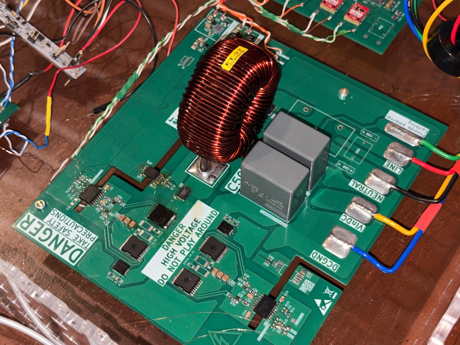
PROJECT CONTEXT & ACADEMIC SCOPE expand_more
CONTEXT: Power Electronics Studio (STU 601), 6th Sem B.Tech EEE, Navrachana University
Role: Primary technical contributor across system design, circuit schematics, component selection, PCB layout, PSIM simulation, and embedded control bring-up.
Status: Custom hardware fabricated; MCU SPWM verified on 100MHz DSO. High-voltage power stage remains unenergized.
Role: Primary technical contributor across system design, circuit schematics, component selection, PCB development, PSIM simulation, and embedded-control bring-up.
Project Status: Custom hardware designed and fabricated; controller-level SPWM verified. Full power-stage operation remains unvalidated.
Project Overview
This project explored the design of a single-phase pure sine wave inverter intended to convert a nominal 72 V DC battery supply into 230 V RMS, 50 Hz AC.
The intended architecture consisted of a front-end DC–DC boost stage to establish a high-voltage DC link, followed by a full-bridge MOSFET inverter controlled using sinusoidal pulse-width modulation (SPWM). The inverter design targeted 20 kHz switching and used an LC output filter to attenuate switching-frequency components.
The work covered power-electronics design, isolated gate driving, auxiliary power distribution, current and voltage sensing, custom PCB development, and embedded control using an STM32G4 microcontroller. PSIM was used to study the inverter's behaviour before physical validation.
The project resulted in a fabricated multi-board prototype and verified controller-level SPWM generation. The front-end boost stage was not completed, and the high-voltage power stage was not energized during testing. Consequently, the intended AC output and rated-load performance remain design and simulation targets rather than demonstrated hardware results.
This dossier documents a comprehensive power-electronics design and prototyping effort with limited hardware validation. Claims of successful operation are strictly confined to controller-level signal generation; power-stage high-voltage switching and 1 kW AC load delivery are presented solely as design targets and simulation outcomes.
Design Targets
The table below records the engineering parameters targeted during the design phase and simulated in PSIM.
Intended standalone battery concept; auxiliary buck designed for this rail.
Designed; simulated in PSIM; unenergized on physical power stage.
Simulated target; not measured on hardware.
Verified in controller modulation envelope on DSO.
Verified on STM32G4 timer outputs with DSO.
Simulated under 1 kW resistive load (52.9 Ω); unvalidated under physical load.
Fabricated multi-layer PCB with CoolMOS C7 switches.
Hand-wound T-57 toroid + dual 2.2 µF Kemet film caps assembled on PCB.
Brought up on custom daughterboard; programmed via SWD.
Full-bridge & rectifier models completed; multi-board system designed & fabricated.
| Parameter | Intended Specification | Implementation & Validation Status |
|---|---|---|
| DC Input | 72 V nominal; approximately 50–80 V intended range | Intended standalone battery concept; auxiliary buck designed for this rail |
| High-Voltage DC Link | Approximately 380–400 V | Designed; simulated in PSIM; unenergized on physical power stage |
| AC Output | 230 V RMS, single-phase | Simulated target; not measured on hardware |
| Output Frequency | 50 Hz | Verified in controller modulation envelope on DSO |
| Switching Frequency | 20 kHz SPWM | Verified on STM32G4 timer outputs with DSO |
| Output Power Target | 800 W continuous / 1 kW peak | Simulated under 1 kW resistive load (52.9 Ω); unvalidated under load |
| Power Topology | Single-phase full-bridge inverter | Fabricated multi-layer PCB with CoolMOS C7 switches |
| Output Filtering | LC low-pass filter | Hand-wound T-57 toroid + dual 2.2 µF Kemet film caps assembled on PCB |
| Digital Controller | STM32G474QET6 (Arm Cortex-M4 @ 170 MHz) | Brought up on custom daughterboard; programmed via SWD |
| Simulation Platform | PSIM | Full-bridge and rectifier simulation models completed |
| PCB Design Tool | KiCad | Multi-board system designed, routed, and manufactured |
Architecture: Intended System vs. Laboratory Arrangement
The project involved two related but distinct architectures: the intended standalone product concept and the laboratory test arrangement created to facilitate studio evaluation.
Intended Standalone Inverter
The original concept was a battery-powered inverter with a nominal 72 V DC input. A front-end boost converter was intended to raise this voltage to approximately 400 V DC, supplying the full-bridge inverter.
Laboratory Arrangement
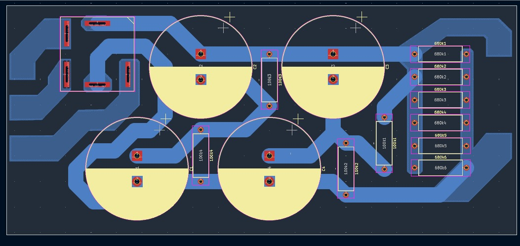
For the academic studio work, a separate three-phase rectifier arrangement was designed to provide a high-voltage DC link from a laboratory AC supply. This allowed the inverter stage to be considered independently of the unfinished battery-input boost converter.
Full-Bridge Power-Stage Design
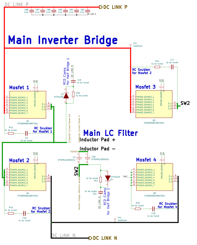
The inverter power stage was designed around four Infineon IPT60R099CM8XTMA1 CoolMOS C7 MOSFETs in a single-phase full-bridge configuration.
-
01
Selection of high-voltage MOSFETs for the intended DC-link voltage: Infineon CoolMOS C7 superjunction silicon was chosen for low area-specific on-resistance (RDS(on) = 99 mΩ) and 600V breakdown voltage, providing breakdown margin above the ~400V DC bus.
-
02
Full-bridge switching topology and associated gate-drive connections: Configured for high-frequency diagonal switching (Q1–Q4, Q2–Q3) to reverse load voltage polarity at 20 kHz carrier frequency.
-
03
PCB routing considerations for switching-current loops and gate-drive returns: Selected the PG-HSOF-8 direct-surface-mount package featuring a dedicated Kelvin driver source pin (
DRIVER_SOURCE) to isolate high-current power return loops from sensitive gate-drive signals and prevent false Miller turn-on. -
04
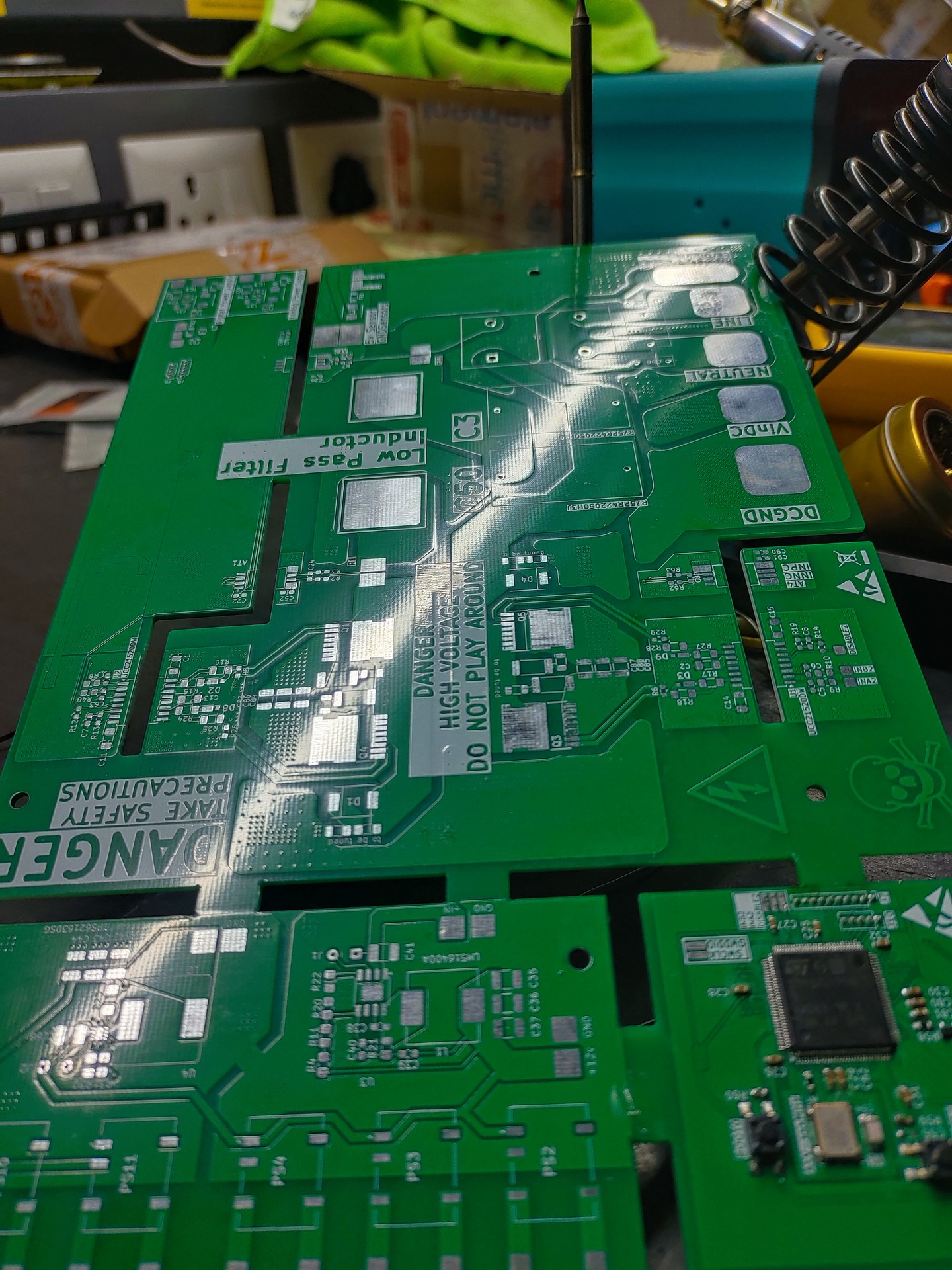
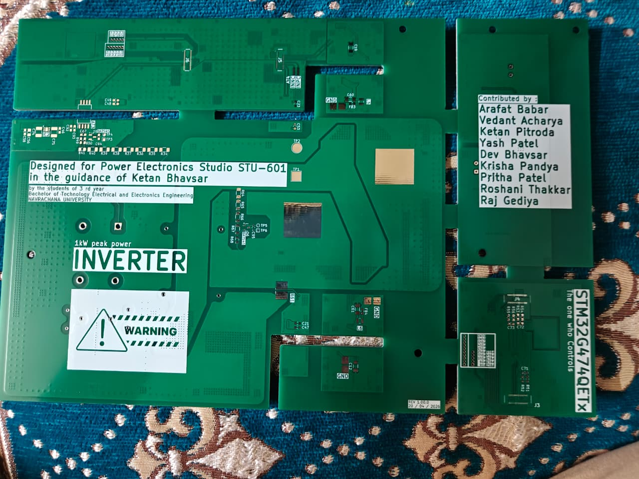
High-voltage isolation spacing and PCB creepage slots: Physical air slots were routed between high-voltage switch nodes and low-voltage control ground planes to maintain dielectric creepage safety.
-
05
Provision for RC snubbers and switch-node clamp circuits: Dedicated footprints for RC snubbers across all 4 switches and ultrafast RCD clamps (STTH310S diodes) across both switch nodes were integrated into the copper layout.
The snubber and clamp component pads were deliberately left unpopulated for later tuning after switching-transient measurements. Since the power stage was not energized, that tuning and its effectiveness were not experimentally established.
Isolated Gate-Drive Architecture
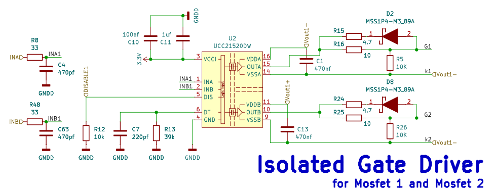
The design used Texas Instruments UCC21520DW isolated gate-driver ICs to interface the low-voltage control system with the MOSFET bridge.
Separate gate-drive channels for the bridge switches with 5.7 kVRMS reinforced galvanic isolation and >100 V/ns common-mode transient immunity (CMTI).
Asymmetric turn-on (10 Ω) and turn-off (4.7 Ω with MSS1P4 Schottky diode) resistor paths to slow down turn-on dv/dt while rapidly discharging gate capacitance.
Dedicated 39 kΩ timing resistors on the UCC21520 DT pins configure a fixed ~390 ns hardware interlock dead-time (tDT ≈ 10 ns × 39 = 390 ns) independently of software execution.
These features were incorporated into the circuit and PCB design. Their presence should not be confused with validation of switching behaviour at the MOSFET gates: the high-voltage power stage was not operated, and the gate-driver output waveforms were not established as verified results.
Auxiliary Power and Sensing
A separate auxiliary power board was designed to distribute power to the control and gate-drive subsystems.
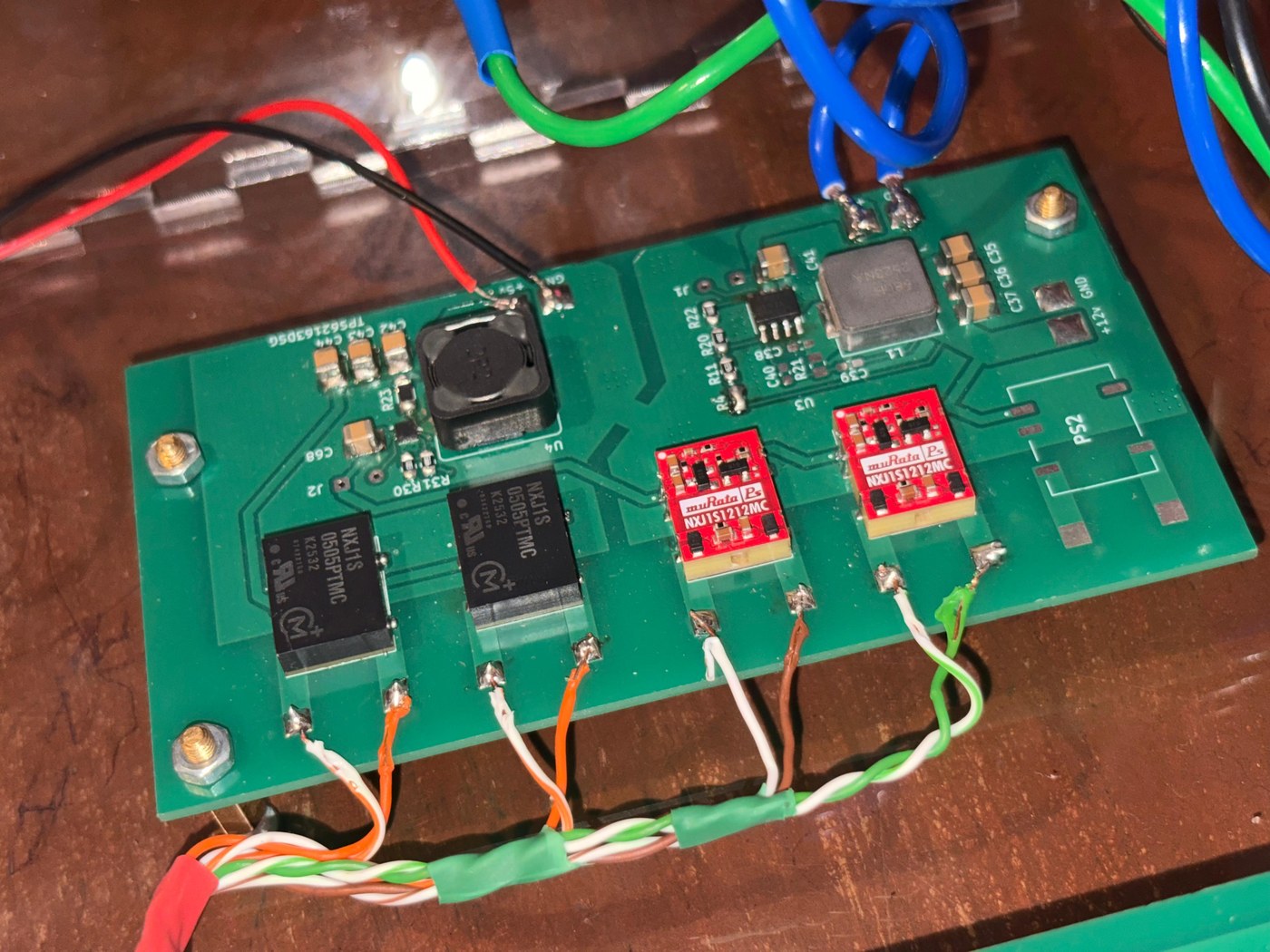
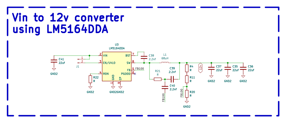
The documented design included a TI LM5164-based input buck stage, a TPS62163-based secondary regulator, and isolated DC–DC converter modules for floating gate-drive and sensing supplies.
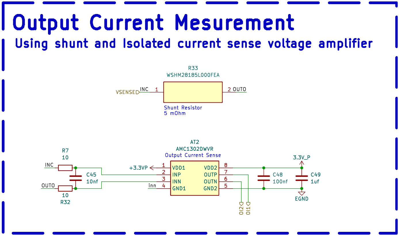
Current measurement was designed around low-value shunt resistors and TI AMC1302 isolated amplifiers. Voltage-sensing networks were also designed to scale high-voltage signals for the control electronics.
Some auxiliary supply rails were measured during bench work, but not every rail was confirmed. The sensing circuits were designed and populated as documented, but calibration and closed-loop feedback operation under load were not validated.
STM32G4 Embedded Control
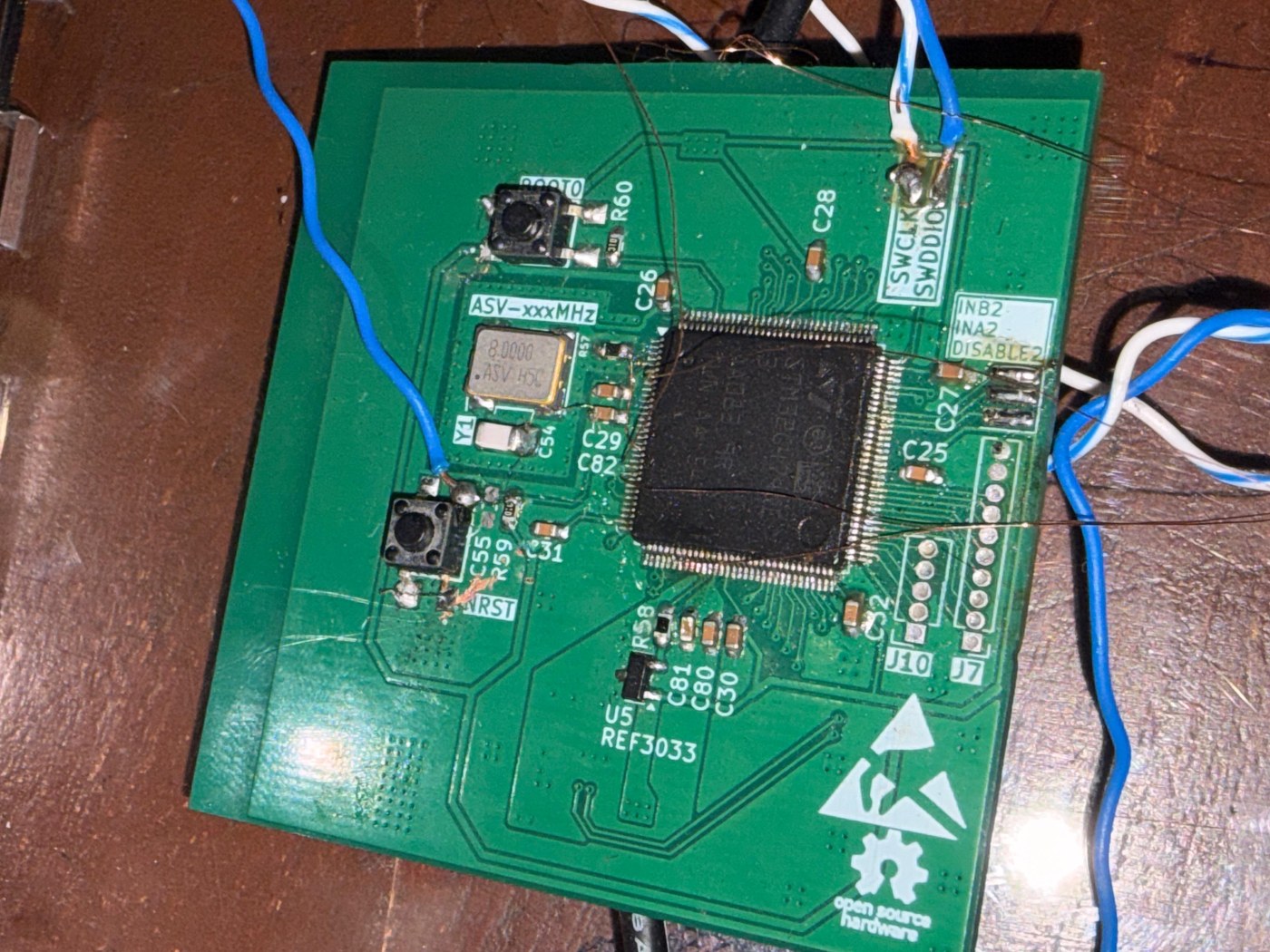
A custom controller board was developed around the STM32G474QET6 microcontroller.
The embedded-control work included configuring the controller for high-resolution PWM generation and producing complementary SPWM signals intended for the full-bridge gate-drive system.
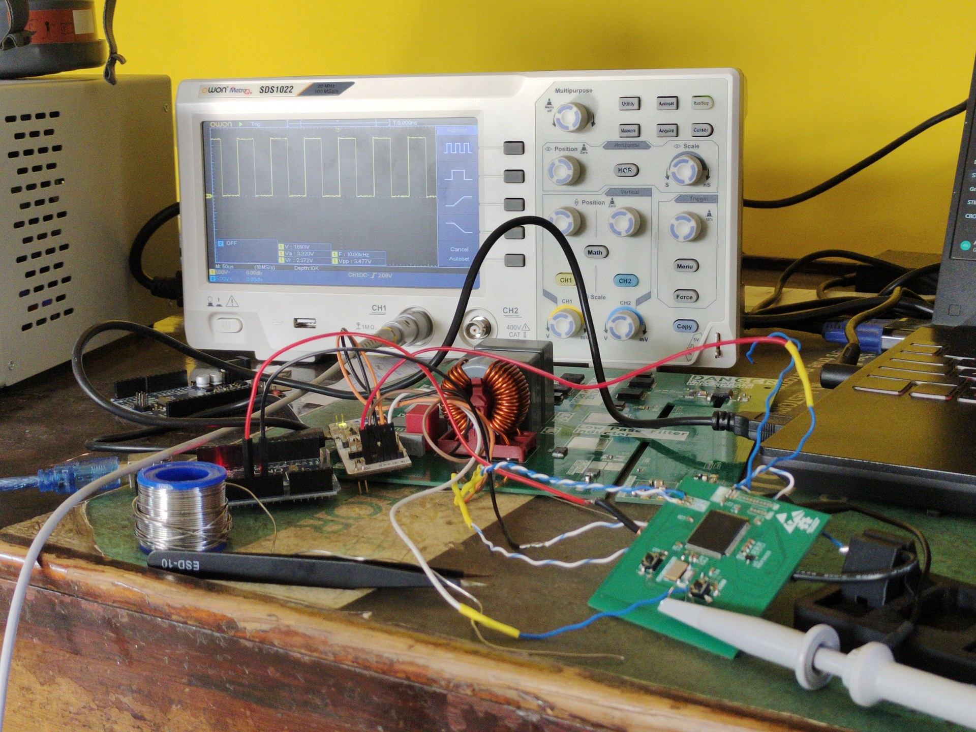
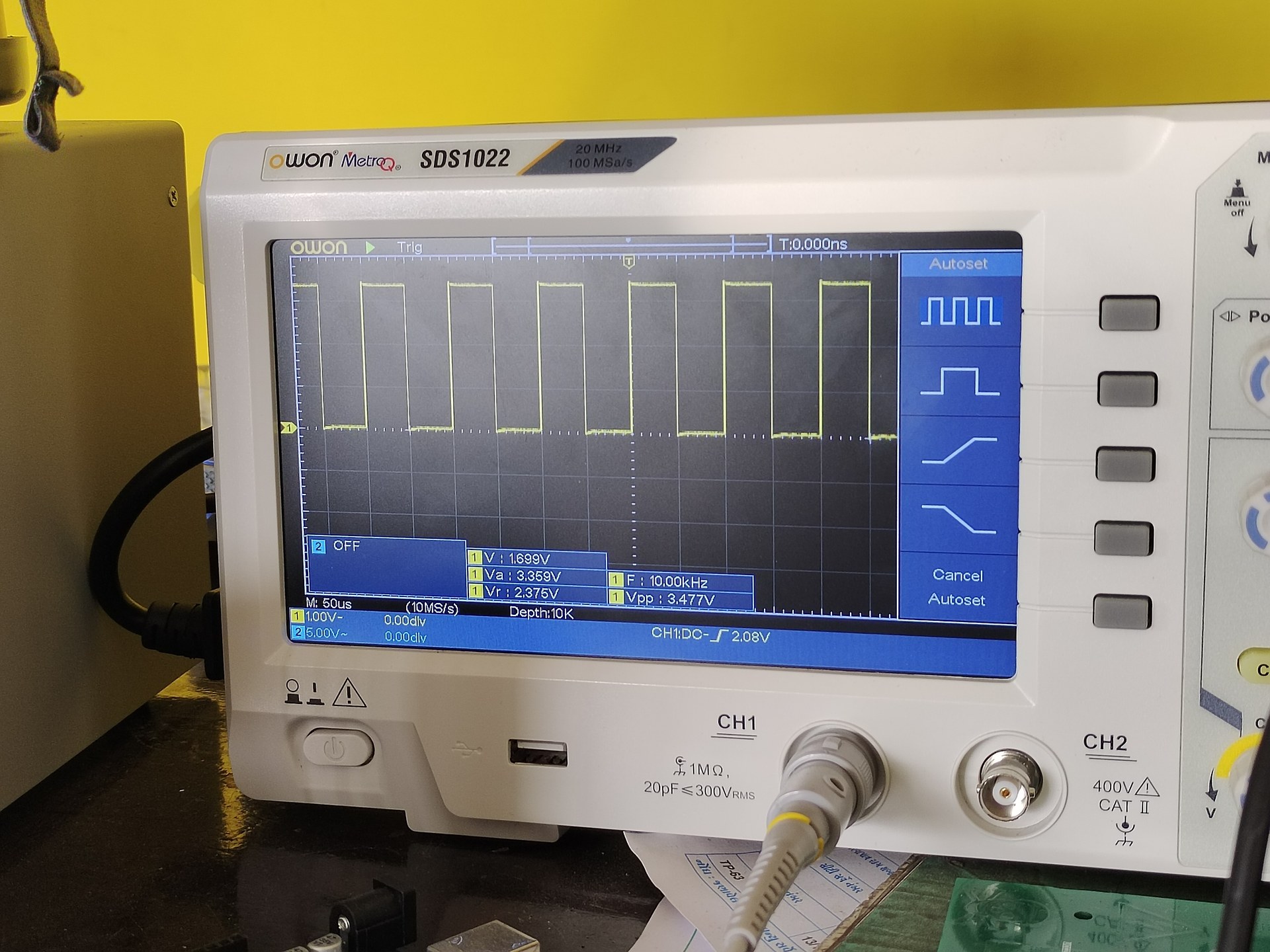
The intended modulation used a 50 Hz sinusoidal reference and a 20 kHz switching carrier. The controller hardware was brought up and programmed, and the generated SPWM signals were observed on a digital storage oscilloscope.
This was the principal confirmed hardware-validation result: controller-level signal generation. It did not demonstrate power conversion, output-voltage regulation, or operation of the complete inverter.
PSIM Simulation
PSIM was used to investigate the inverter topology and output-filter behaviour before physical testing.
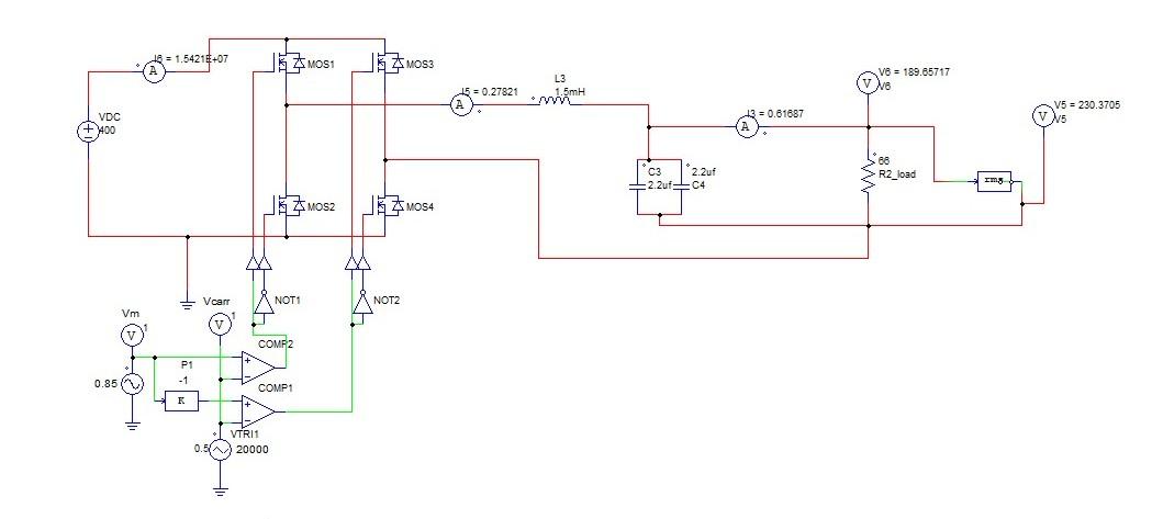
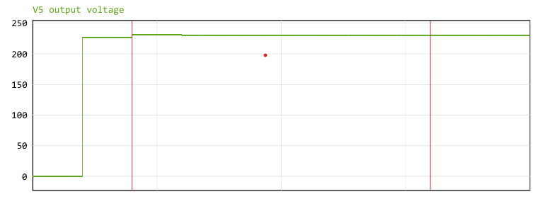
The report presents simulated operation targeting a 230 V RMS, 50 Hz output with a 1 kW resistive load. These results belong to the simulation environment and must be labelled accordingly. No corresponding 230 V AC output or 1 kW load test was completed on the physical prototype.
Prototype and Validation Status
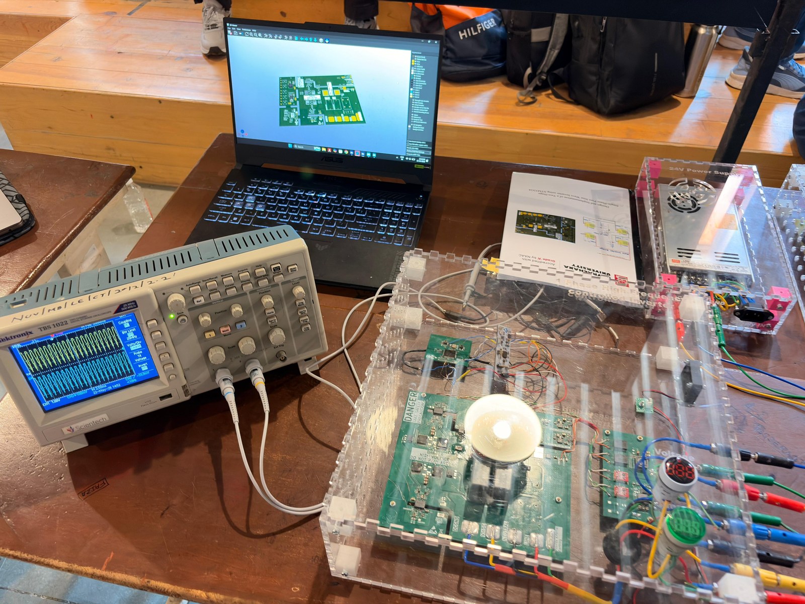
The work progressed beyond simulation into physical electronics development. Custom PCBs were fabricated, the controller was assembled and brought up, and SPWM generation was verified at the control-signal level.
Fabricated and assembled, according to the hardware audit.
Brought up; SPWM generation verified on 100 MHz DSO.
Fabricated; some rails measured during bench testing.
Driver chips populated; high-voltage gate switching not confirmed.
Not completed in hardware during the project period.
Power stage was not energized at ~400V DC during testing.
Sensing circuits routed; closed-loop feedback unvalidated on hardware.
Simulation target in PSIM; not measured on physical hardware.
No physical 1 kW power-stage load test was conducted.
No power-analyzer measurements exist.
Pads marked "to be tuned" pending switching-transient measurements.
| Subsystem | Status | Verification Notes |
|---|---|---|
| Inverter power-stage PCB | Fabricated & Assembled | Fabricated and assembled, according to the hardware audit |
| STM32G4 controller | Verified (Signal-Level) | Brought up; SPWM generation verified on 100 MHz DSO |
| Auxiliary power board | Fabricated | Fabricated; some rails measured during bench testing |
| Gate-driver output operation | Not Confirmed | Driver chips populated; high-voltage gate switching not confirmed |
| Front-end boost converter | Not Completed | Not completed in hardware during the project period |
| High-voltage DC-link switching | Not Tested | Power stage was not energized at ~400V DC during testing |
| Closed-loop output regulation | Not Validated | Sensing circuits routed; closed-loop feedback unvalidated on hardware |
| 230 V RMS output | Simulation Target | Simulation target in PSIM; not measured on physical hardware |
| Rated-load operation | Not Tested | No physical 1 kW power-stage load test was conducted |
| Efficiency and output THD | Not Measured | No power-analyzer measurements exist |
| Snubber and clamp tuning | Pending Tuning | Pads marked "to be tuned" pending switching-transient measurements |
My Technical Contribution
My primary contribution was the engineering design and development work rather than report writing.
System architecture and power-conversion topology selection, including full-bridge superjunction configuration, 20 kHz switching trade-offs, and auxiliary multi-rail distribution.
Component selection and circuit schematic design across the inverter power stage, UCC21520 gate drivers, LM5164 buck converter, and AMC1302 isolated sensing networks.
PCB design and development for the power stage, auxiliary supplies, and controller boards, implementing creepage cutouts, Kelvin source routing, and ground-plane isolation.
PSIM modelling and simulation of the full-bridge inverter, LC harmonic filter, three-phase rectifier stage, and 1 kW load behavior.
STM32G4 controller development, clock tree configuration with external active crystal, and High-Resolution Timer (HRTIM) SPWM pulse generation with complementary dead-time.
Hardware bring-up and oscilloscope-based signal verification, capturing complementary SPWM modulation waveforms and verifying driver timing.
Integration planning across power electronics, sensing, auxiliary supplies, and embedded control to establish a clean modular development pipeline.
Engineering Reflection
One of my biggest takeaways from this project was realising that designing a system is often easier than testing it in the real world.
Simulation can help establish whether an approach is theoretically sound, but physical hardware introduces another level of uncertainty. In power electronics, a decision about a component, circuit architecture, or PCB layout can affect fabrication costs, debugging effort, and the time required for another revision.
The experience made me appreciate the importance of evaluating engineering decisions carefully before committing them to hardware.
“A design is a hypothesis until it has been validated against reality.”
Next Engineering Steps
The next stage of development would focus on closing the gap between design and experimental validation: